TOP
Services
Services
Services
Solutions
Extended Path: From Technology to Complete Solutions
- Solutions
Copper Pillar Module
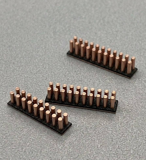
Copper Pillar Module Solution
CORE VALUE
Core Advantages
SPEED
Fast Integration
COST
Cost Efficiency
FLEXIBILITY
Flexible Customization
POSITIONING
Industry Applications & Strategic Positioning
Compared to traditional solder balls and wafer-level copper pillar processes, here is how modular solutions position themselves in terms of adoption barriers and flexibility:
| Feature | Traditional Solder Ball | Copper Pillar Bump (Wafer-Level Process) |
Copper Pillar Module (Modular Solution) |
Business Value |
|---|---|---|---|---|
| Interconnect Density | Limited by solder ball size — large pitch, low density | High Density (Fine Pitch) | High Density (Fine Pitch) | Meets high-frequency signal transmission requirements |
| Electrical Performance | High resistance and inductance | High Density (Fine Pitch) | High Density (Fine Pitch) | Meets high-frequency signal transmission requirements |
| Process Structure | Flexible solder balls, prone to collapse | Rigid structure, dimensionally stable | Rigid structure + integrated molding support | High reliability, controlled stacking height |
| Infrastructure | Standard packaging line | Requires high-end wafer electroplating Fab (High Capex) Capex) |
Works on existing SMT production lines | Extremely low adoption barrier, fast mass production |
| Design Flexibility | Primarily standardized mass production | Limited by equipment electroplating height | Highly flexible, fully customized service | Meets specific R&D and application requirements |

POSITIONING
Key Technical Breakthrough:
Precise Height Control & Packaging Reliability
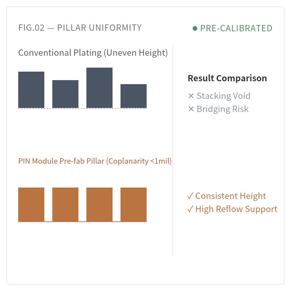
The biggest challenge for customers is height uniformity constraints with electroplated copper pillars, leading to voids or bridging during stacking. Modular technology uses pre-fabricated pillars combined with high-precision curing adhesive — no reliance on real-time electroplating growth.
- Precise Height — Modules are height-calibrated before shipment, eliminating variation from the electroplating process.
- Structural Stability — Curing adhesive provides better support than traditional Underfill after reflow, preventing solder cracking caused by CTE mismatch.
SOLUTION SELECTOR
Product Line Selector
G1
Copper Pillar Module
Pin module
G3
Integrated Molding Module
molding interposer pin module
G4/G5
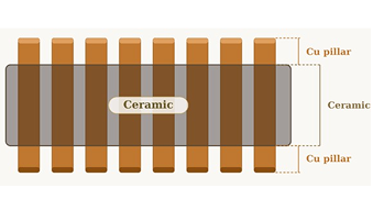
Ceramic Solution
Ceramic Molding Interposer Pin
WHERE IT FITS
Application Scenarios
01
AI Servers & High-Performance Computing
AI SERVER / HPC
Pain Points
Entry Points
Recommended Series
02
Power Semiconductor Modules
POWER MODULE / SiC・GaN
Pain Points
Entry Points
Recommended Series
03
Consumer Electronics SiP Modules
WEARABLES / MOBILE SiP
Pain Points
Entry Points
Recommended Series
04
Automotive Electronics
AUTOMOTIVE ELECTRONICS
Pain Points
Entry Points
Coplanarity < 1mil (better than JEDEC standards), combined with full-line AOI inspection, meets automotive demands for consistency and traceability.
Recommended Series
05
RF / Millimeter-Wave Modules
RF & mmWave MODULES
Pain Points
Entry Points
Recommended Series
DATASHEET
Technical Specifications
Process Specifications
Center Pitch
Inspection Standard
FAQ
Technical Q&A
Why Choose Copper Pillar Modules Over Traditional Solder Balls?
How does this differ from Copper Pillar Bump (wafer-level process)?
How does this differ from Copper Pillar Bump (wafer-level process)? - Process Barrier — Copper Pillar Bumps must be fabricated in a semiconductor fab using expensive masks and electroplating equipment with enormous capex. Modules standardize copper pillar technology into a component format, enabling equivalent high-density interconnects on standard SMT lines.
- Flexibility & Cycle Time — The Bump process is extremely unfriendly to small batches or diverse designs with long lead times. Modules support fully customized heights and layouts, enabling rapid prototyping without millions in wafer mask costs.
- Structural Support — Modules combine integrated molding and curing adhesive technology, providing better mechanical support than bare bumps, effectively solving warpage issues in large-format packages.
Can my existing SMT line mount these directly? Is special Flip-Chip equipment required?
How do you overcome stacking height limitations and electroplating uniformity constraints?
How do you overcome stacking height limitations and electroplating uniformity constraints? Ready to Validate Your Packaging Design?
G1 / G3 / G4-G5 sample prototyping available.
Customized configuration recommendations based on your XPU and substrate specifications.