

TOP
Services
Services
Services
- STRUCTURAL R&D · PITCH 0.13MM → 0.08MM
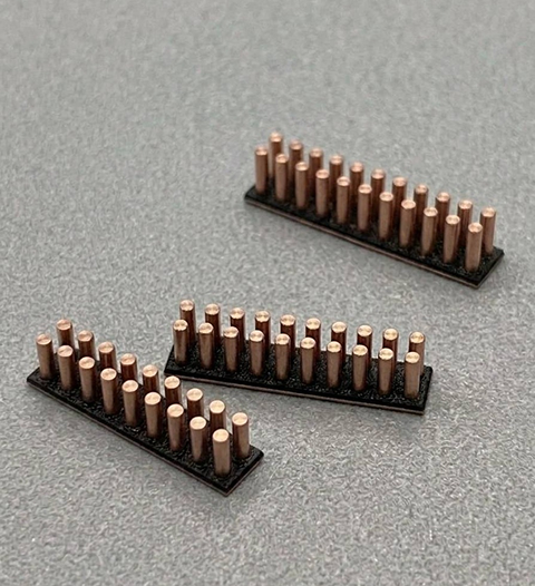
Copper Pillar Module — High Current Line
Redefining the Physical Limits of Connectors into Negotiable Specifications.
The industry’s mass-production standard stops at 0.13mm pitch. We treat miniaturization as a structural engineering problem, not a process slogan — using materials science, tolerance control, and a modular platform to turn extreme customization into a scalable service.
Products on the market commonly fail at three structural failure points during extreme miniaturization: fragile solder joints, impedance mismatch, and contact failure caused by assembly tolerances. Our solution is designed from these three failure factors backward.


THE PROBLEM
Industry Trends & Thermal Challenges
Product Core Value
Redefining the Physical Limit
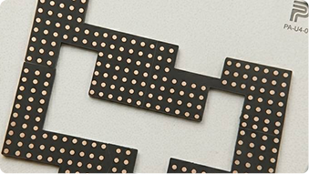
Beyond the industry’s 0.13mm pitch mass-production standard, we offer extreme customization services down to 0.08mm pitch through proprietary materials and manufacturing processes — pushing the boundaries of spatial layout rather than stopping at the edge of a spec sheet.
Full-Dimension Customization
Not just pin count and length — we also cover shape and total thickness. We engage in structural design from the PCB layout stage, achieving seamless integration of housing and components.
From Manufacturer to Structural Consultant
Input your space constraints, signal frequency, and expected volume, and we return feasible structural recommendations — advancing our service positioning from a simple parts supplier to a structural consultancy.
PAIN-POINT MAPPING
Pain-Point Mapping
Every side effect of miniaturization corresponds to a specific, verifiable engineering countermeasure — not a marketing guarantee.
| Market Pain Point | Our Countermeasure |
|---|---|
|
⊘Miniaturization leads to structural fragility
|
→High-strength alloy + optimized geometry
Redistributing stress paths to enhance overall physical strength margins at the same pin diameter.
|
|
⊘Miniaturization leads to structural fragility
|
→Intelligent modular process
Maintaining high consistency in mass production through ultra-tight tolerance control, rather than relying on manual selection of good parts.
|
|
⊘High customization leads to long development cycles
|
→Intelligent modular process
Maintaining high consistency in mass production through ultra-tight tolerance control, rather than relying on manual selection of good parts.
|
|
⊘Ultra-fine pitch affects electrical performance
|
→Advanced signal integration technology
Minimizing interference and impedance mismatch, ensuring miniaturization doesn't come at the cost of signal integrity.
|
Structured Strategy and Risk Management
Universal Base + Customizable Terminals
The base maintains equipment commonality and yield benchmarks; only the terminal module is replaced to match customer space constraints and signal specifications — allowing “extreme customization” without sacrificing mass production economics.
Failure Factors & Risk Mitigation
| Potential Failure Factor | Risk Mitigation Strategy |
|---|---|
| Over-miniaturization → Insufficient mechanical rigidity → Reduced assembly yield | Introduce thermal stress and mechanical fatigue simulation (FEA) at the design stage to eliminate physical failure points before prototyping. |
| Overly complex customization requirements → Inability to scale | Universal base + customizable terminal logic maintains core production equipment commonality; customization occurs only in local modules. |
DESIGN RULES
DESIGN RULES — Pitch 0.13mm – 0.08mm
| Pitch Range | Recommended Pin Diameter | Design Tolerance (mm) | Key Application | Classification |
|---|---|---|---|---|
| 0.130 - 0.110mm | φ 0.09 - 0.15mm | Low | Standard SiP / Wearables | Standard |
| 0.110 - 0.095mm | φ 0.08 - 0.12mm | Medium | Standard SiP / Wearables | Optimized |
| 0.095 - 0.080mm | φ 0.06 - 0.09mm | High (FEA required) | 2.5D/3D IC, HBM Advanced Integration | Extreme Custom |
Three-Tier Quotation Structure
STRATEGIC VALUE
Future Business Roadmap
Think of connectors as an “invisible” presence — not just connectivity, but as an integral part of the PCB structure.
| NOW |
Customization Assessment Checklist
Redistributing stress paths to enhance overall physical strength margins at the same pin diameter.
|
| NEXT |
5G/6G and HPC Impedance Control Standards
Align in advance with the impedance control specifications required for high-speed computing scenarios for high-frequency transmission needs, positioning for the next wave of high-margin markets.
|
| HORIZON |
Connector-less Transfer Solution
As customers gradually move toward connector-PCB integration, PCB prepare structural transition paths in advance to allow existing product lines to smoothly connect to next-generation design trends.
|
FAQ
Technical Q&A
Why use Copper Pillar Module instead of traditional Solder Balls?
Why use Copper Pillar Module instead of traditional Solder Balls? Traditional solder balls are limited by surface tension, resulting in larger pitch and susceptibility to collapse. Copper pillar modules provide finer pitch and shorter conduction paths, significantly reducing resistance and inductance to meet the demands of modern AI and high-performance computing (HPC) for signal integrity and power delivery.
How does this differ from the industry-standard Copper Pillar Bump (wafer-level process)?
How does this differ from the industry-standard Copper Pillar Bump (wafer-level process)? 1. Process Barrier | Bump requires costly masks and electroplating equipment at semiconductor fabs with enormous Capex; our module standardizes copper pillar technology so equivalent high-density interconnects can be achieved at standard SMT facilities.
2. Flexibility & Lead Time | Bump process is unfriendly to low-volume or diversified designs with long lead times; modules support fully customized heights and arrays, with fast prototyping and no multi-million wafer mask costs.
3. Structural Support | Modules combine one-piece molding and thermosetting adhesive for better mechanical support than bare bumps, effectively resolving warpage issues in large-format packages.
Can my SMT line place components directly? Do I need special Flip-Chip equipment?
Can my SMT line place components directly? Do I need special Flip-Chip equipment? Yes, this is the core value proposition. The module has excellent SMT compatibility — no need to purchase expensive wafer alignment machines. Through calculated Pad compensation (+50–100μm), it perfectly absorbs Tilt and Offset errors during assembly, achieving precise high-volume placement with your existing high-speed pick-and-place machines.
How to overcome the limitations of stack height and plated copper pillar uniformity?
How to overcome the limitations of stack height and plated copper pillar uniformity? Traditional Copper Pillar Bump electroplating often has height variations between the wafer edge and center, causing voids or open circuits during stacking. Our “Pre-fabricated Pillar” technology ensures each pillar is precisely height-calibrated before shipment (coplanarity < 2mil), fundamentally compensating for the physical limitations of electroplating equipment and ensuring absolutely consistent height after stacking.