TOP
Services
Services
Services
- WAFER-LEVEL COPPER PILLAR INTERCONNECT
Breaking the 3D Wafer Stacking Limit:
High-Density Pin Module on Wafer Solution
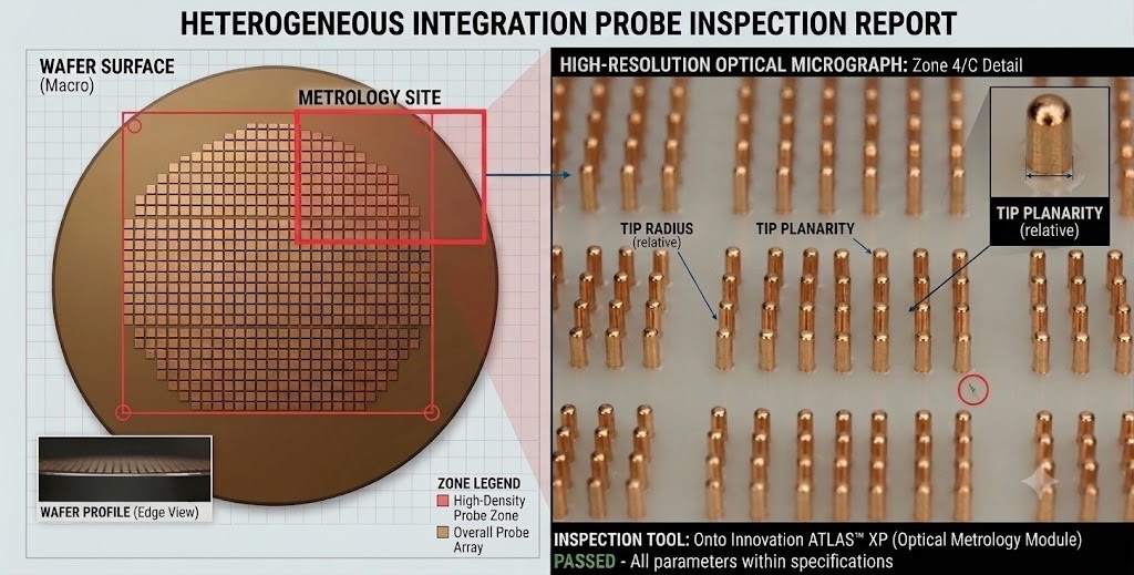
300,000 copper pillars on a single 8″ wafer, placed in one operation at 99.9% yield — unlocking the physical bottleneck of next-generation advanced packaging.
300,000
+
Copper pillars per 8" wafer
99.9
%
Current process yield (targeting 99.99%)
>150
°C
Automotive-grade thermal resistance

THE PROBLEM
Why Are Traditional Stacking Solutions Failing?
As 3D IC and multi-chip module (MCM) stacking heights increase, traditional solder bumps face the following physical limitations:
Pitch Limitation
Solder bumps tend to flow laterally during high-temperature reflow, limiting the improvement of interconnect density.
Stress Failure
Mismatched thermal expansion coefficients (CTE) between wafers cause fractures at the stacking interface under high-temperature vibration.
Electrical Bottleneck
High impedance of tin alloys fails to meet future ultra-high-speed transmission and thermal dissipation requirements.
DATASHEET
Product Specifications & Features
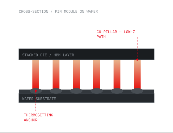
We directly implant micro copper pillars into the wafer, providing the shortest, lowest-impedance vertical electrical pathways.
Thermosetting Anchor Technology
A high-stability thermosetting adhesive is applied at the base of each copper pillar. After high-temperature curing, it forms an irreversible three-dimensional cross-linked structure providing excellent mechanical strength and heat resistance, firmly locking all 300,000 copper pillars in position and perfectly overcoming stress and warpage issues in subsequent stacking processes.

Application Scenarios
Outstanding Performance & Technical Specifications
| Specification | Details |
|---|---|
| High-Density Placement | 300,000 copper pillars per 8" wafer |
| Exceptional Yield | 99.9% (target 99.99%) |
| Thermal & Structural Stability | No shift or delamination through multiple high-temperature reflow cycles |
| Bonding Method | High-stability thermosetting adhesive base / Three-dimensional cross-linked structure |
| Applicable Wafer Size | 8 inch (other sizes evaluated upon request) |
APPLICATION SCENARIOS
Core Application Scenarios
We pursue not only high yield, but proactively prevent all potential failure factors early in the process, ensuring a flawless product introduction:
01
Preventing Incomplete Adhesive Curing
We employ Dynamic Scanning Calorimetry (DSC) testing to ensure the crosslink degree of every adhesive batch exceeds 95%, completely eliminating voids and fractures caused by high-temperature outgassing.
02
Preventing Copper Pillar Oxidation
The entire process is performed under an oxygen-free nitrogen (N₂) atmosphere with plasma cleaning, ensuring all 300,000 contacts maintain extremely low contact resistance.
SELF-SERVICE ASSESSMENT
Quick Technical Assessment Guide
Is Pin Module technology right for you? Please refer to the following criteria:
If any of the above answers is “Yes,” Pin Module will be your best solution.
FAQ
Technical Q&A
Why use Copper Pillar Module instead of traditional Solder Balls?
Why use Copper Pillar Module instead of traditional Solder Balls? Traditional solder balls are limited by surface tension, resulting in larger pitch and susceptibility to collapse. Copper pillar modules provide finer pitch and shorter conduction paths, significantly reducing resistance and inductance to meet the demands of modern AI and high-performance computing (HPC) for signal integrity and power delivery.
How does this differ from the industry-standard Copper Pillar Bump (wafer-level process)?
How does this differ from the industry-standard Copper Pillar Bump (wafer-level process)? 1. Process Barrier | Bump requires costly masks and electroplating equipment at semiconductor fabs with enormous Capex; our module standardizes copper pillar technology so equivalent high-density interconnects can be achieved at standard SMT facilities.
2. Flexibility & Lead Time | Bump process is unfriendly to low-volume or diversified designs with long lead times; modules support fully customized heights and arrays, with fast prototyping and no multi-million wafer mask costs.
3. Structural Support | Modules combine one-piece molding and thermosetting adhesive for better mechanical support than bare bumps, effectively resolving warpage issues in large-format packages.
Can my SMT line place components directly? Do I need special Flip-Chip equipment?
Can my SMT line place components directly? Do I need special Flip-Chip equipment? Yes, this is the core value proposition. The module has excellent SMT compatibility — no need to purchase expensive wafer alignment machines. Through calculated Pad compensation (+50–100μm), it perfectly absorbs Tilt and Offset errors during assembly, achieving precise high-volume placement with your existing high-speed pick-and-place machines.
How to overcome the limitations of stack height and plated copper pillar uniformity?
How to overcome the limitations of stack height and plated copper pillar uniformity? Traditional Copper Pillar Bump electroplating often has height variations between the wafer edge and center, causing voids or open circuits during stacking. Our “Pre-fabricated Pillar” technology ensures each pillar is precisely height-calibrated before shipment (coplanarity < 2mil), fundamentally compensating for the physical limitations of electroplating equipment and ensuring absolutely consistent height after stacking.