TOP
Services
Services
Services
- CMOS / PCB WARPAGE SOLUTION
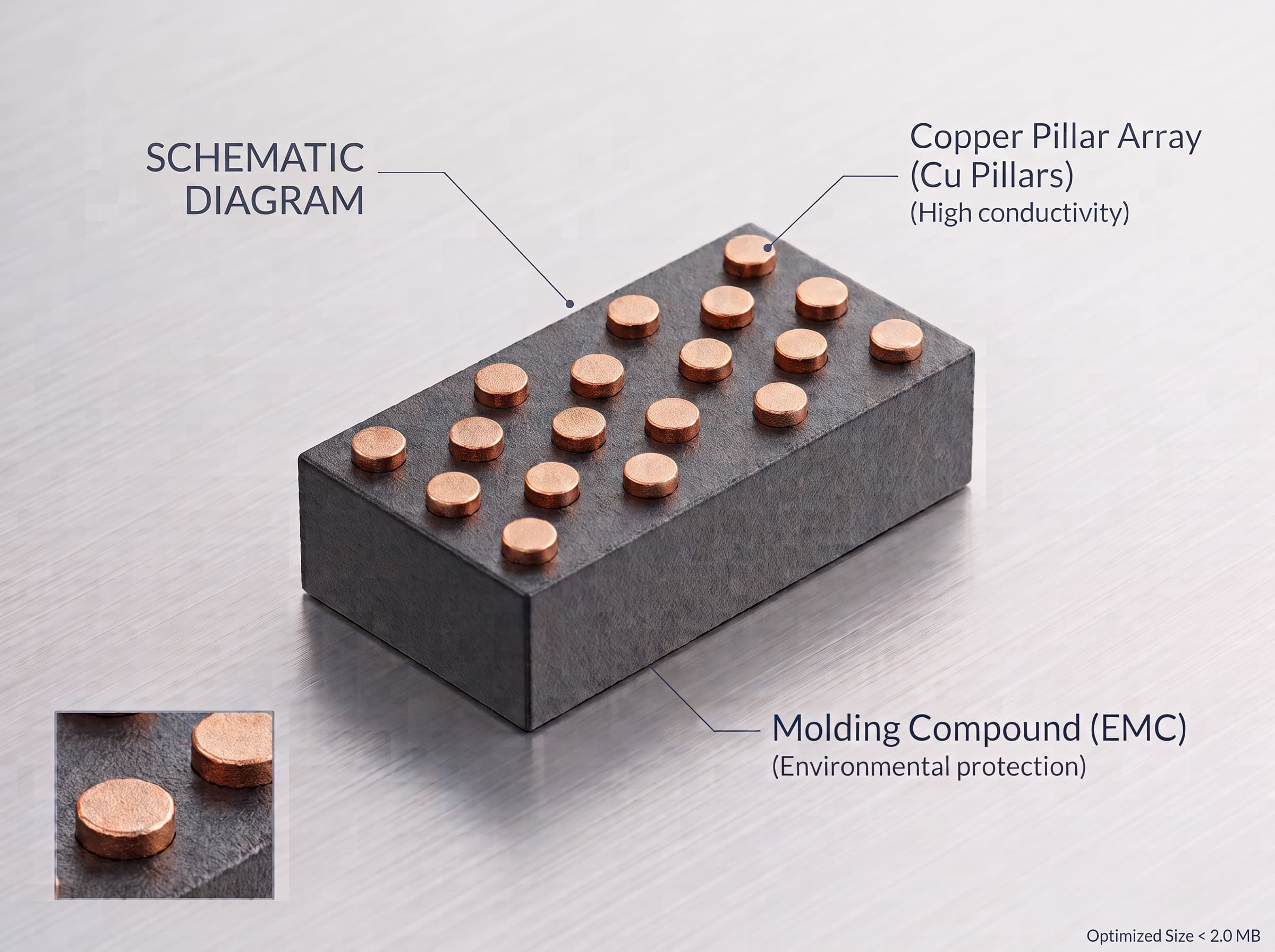
One Copper Pillar,
Simultaneously Solving Stress, Optics, Electrical & Thermal
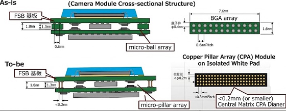
Due to inconsistent material thermal expansion coefficients, CMOS image sensor modules are highly susceptible to warpage during SMT reflow, causing solder ball voids and micro-cracks. iPin’s advanced copper pillar technology starts from the structural root, offering an integrated all-in-one solution.
4-in-1
Stress / Optics / Electrical / Thermal
Cu
High-Conductivity Pure Copper Pillar
Custom
Fully Customizable Height Design
CMOS Warpage Integration Solution
iPin Advanced Copper Pillar Technology

THE PROBLEM
About CMOS IC Warpage
CMOS IC warpage refers to the bending deformation of a chip during manufacturing or SMT board soldering, caused by differing thermal expansion coefficients (CTE) between materials. When IC packages and PCBs are heated in the high-temperature reflow oven of surface mount technology (SMT), different materials expand at different rates, creating internal stress and bending upon cooling.
This leads to solder ball voids, cold joints, or micro-cracks, causing premature product failure. This is especially pronounced in advanced packaging or thin wafer applications, where heterogeneous integration and wafer thinning make stress imbalance between layers more likely. When warpage exceeds 0.75%, soldering defects are highly likely.
Now, simply using our iPin perfectly resolves this warpage pain point.

Core Advantages and Solutions of IPIN Products
Four Core Advantages — Integrated All-in-One Solution
| No. | Core Advantage | Technical Description |
|---|---|---|
| 01 |
Warpage Control
Warpage Control
|
The iPin metal pillar structural design dynamically helps distribute interface stress, significantly reducing warpage, fundamentally preventing soldering defects from high-temperature reflow and resolving chip deformation and solder void issues. |
| 02 |
Height Adjustment
Height Adjustment
|
iPin height can be fully customized per customer requirements, precisely ensuring perfect consistency in the gap between lens and photosensitive surface, significantly improving optical module mass production yield. |
| 03 |
Electrical Connection
|
iPin can be used directly as a highly conductive pillar, providing ultra-low impedance, high-frequency stable signal transmission and key grounding capability, ensuring image signals are noise-free and undistorted. |
| 04 |
Thermal Dissipation
Thermal Dissipation
|
iPin uses high-thermal-conductivity copper, efficiently conducting heat to the PCB heat dissipation layer via the shortest path, significantly improving sensor thermal stability and service life. |
Why choose iPin?
Why Choose iPin?
| Item | Value Description |
|---|---|
| 01 — Integrated Solution | One component simultaneously solves four major pain points: stress deformation, optical tolerance, electrical transmission, and core thermal dissipation. |
| 02 — Process Optimization | Reduces time and cost of repeatedly modifying substrate designs due to material mismatch, accelerating time-to-market. |
| 03 — Quality Protection | Eliminates solder ball cold joints and micro-cracks, significantly reducing early failure rates after product shipment. |
FAQ
Technical Q&A
Why use Copper Pillar Module instead of traditional Solder Balls?
Why use Copper Pillar Module instead of traditional Solder Balls? Traditional solder balls are limited by surface tension, resulting in larger pitch and susceptibility to collapse. Copper pillar modules provide finer pitch and shorter conduction paths, significantly reducing resistance and inductance to meet the demands of modern AI and high-performance computing (HPC) for signal integrity and power delivery.
How does this differ from the industry-standard Copper Pillar Bump (wafer-level process)?
How does this differ from the industry-standard Copper Pillar Bump (wafer-level process)? 1. Process Barrier — Bump requires costly masks and electroplating equipment at semiconductor fabs with enormous Capex; our module standardizes copper pillar technology so equivalent high-density interconnects can be achieved at standard SMT facilities.
2. Flexibility & Lead Time — Bump process is unfriendly to low-volume or diversified designs with long lead times; modules support fully customized heights and arrays, with fast prototyping and no multi-million wafer mask costs.
3. Structural Support — Modules combine one-piece molding and thermosetting adhesive for better mechanical support than bare bumps, effectively resolving warpage issues in large-format packages.
Can my SMT line place components directly? Do I need special Flip-Chip equipment?
Can my SMT line place components directly? Do I need special Flip-Chip equipment? Yes, this is the core value proposition. The module has excellent SMT compatibility — no need to purchase expensive wafer alignment machines. Through calculated Pad compensation (+50–100μm), it perfectly absorbs Tilt and Offset errors during assembly, achieving precise high-volume placement with your existing high-speed pick-and-place machines.
How to overcome the limitations of stack height and plated copper pillar uniformity?
How to overcome the limitations of stack height and plated copper pillar uniformity? Traditional Copper Pillar Bump electroplating often has height variations between the wafer edge and center, causing voids or open circuits during stacking. Our “Pre-fabricated Pillar” technology ensures each pillar is precisely height-calibrated before shipment (coplanarity < 2mil), fundamentally compensating for the physical limitations of electroplating equipment and ensuring absolutely consistent height after stacking.